TSMC has been offering foundry services since 1987, and their first 3nm node was called N3 and debuted in 2022; now they have an enhanced 3nm node dubbed N3E that has launched. Every new node then requires IP that is carefully designed, characterized and validated in silicon to ensure that the IP specifications are being met and can be safely used in SoC designs. This new IP must cover a wide range of functions, like interface, memory and logic. Synopsys has a large IP team that has risen to the challenge by creating new IP for the TSMC N3E node and achieving first-pass silicon success.
Chiplet Interconnect
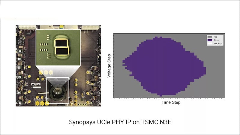
Systems made up of chiplets require die-to-die communication, and that’s where the UCIe standard comes into play. Synopsys is a Contributor member of the UCIe Consortium, and they offer IP for both a UCIe Controller and a UCIe PHY in the TSMC N3E node.

The UCIe PHY IP had first silicon results in August 2023, showing data rates of 16GB/s and scalable to 24GB/s per channel. Power efficiency is at 0.3 pJ/bit.
PHY IP
The IEEE approved the 802.3 standard for Ethernet back in 1983, quite the extended standard, while the Synopsys 224G Ethernet PHY IP had first silicon success in August 2023. Network engineers look at the eye diagram to see the PAM-4 encoding. Jitter levels surpassed both the IEEE 802.3 and OIF standard specifications.

Supporting standards like PCI Express 6.0, 400G/800G Ethernet, CCIX, CXL2.0/3.0, JESD204 and CPRI there is the Synopsys Multi-Protocol 112G PHY IP. Engineers can combine this PHY IP with a MAC and PCS to build a 200G/400G/800G Ethernet block.

SDRAM and memory modules can use the Synopsys DDR5 PHY IP on TSMC N3E to achieve transfer rates up to 8400Mbps. You can see the wide open eye and clear margins for this IP operating at speed.

The PCI Express standard started out in 2003 and has been continually updated to meet the growing demands of cloud computing, storage and AI. PCIe 5.0 is now supported using the Synopsys PCIe 5.0 PHY IP. First silicon on TSMC N3E showed operating speeds of 32 GT/s, and it passed the compliance testing.

I’ve been using USB-C on my MacBook Pro, iPad Pro and Android phone for years now. Synopsys now supports USB-C 3.2 and DisplayPort 1.4 PHY IP in the latest TSMC process. With this IP users can connect up to 8K Ultra High Definition displays.
")
Smartphone companies standardized on the MIPI protocol years ago as an efficient way to connect cameras, and the Synopsys MIPI C-PHY IP/D-PHY IP can operate at 6.5Gb/s per lane and 6.5Gs/s per trio. The C-PHY IP supports v2.0, and the D-PHY IP2.1.

The latest Synchronous DRAM controller spec is LPDDR5X, supporting data transfer speeds up to 8533Mbps, a 33% improvement over LPDDR5 memory. The Synopsys LPDDR5X/5/4X Controller is silicon-proven, and ready to be designed with.

Logic Libraries and Memories
Up to half the area of an SoC can be memories, so the good news is that the Synopsys Foundation IP allows you to add memories and logic library cells quickly into a new design. Here are the test chip diagrams from Synopsys on the TSMC N3E node for memories and logic libraries.

Summary
TSMC and Synopsys have collaborated quite well together over the years, and that partnership now extends to the N3E node where SoC designers can find silicon-tested IP for interfaces, memories and logic. Power, performance and yield are looking attractive for N3E, so the technology is ready for your most demanding designs. Starting a design with N3E also provides you a quicker path to migrate to the N3P process.
Instead of creating all of your own IP from scratch, which will lengthen your schedule, require more engineering resources and increase risk, why not take a look at what Synopsys has to offer in a wide range of IP blocks that are silicon-proven.
Related Blogs
Share this post via:
- SEO Powered Content & PR Distribution. Get Amplified Today.
- PlatoData.Network Vertical Generative Ai. Empower Yourself. Access Here.
- PlatoAiStream. Web3 Intelligence. Knowledge Amplified. Access Here.
- PlatoESG. Carbon, CleanTech, Energy, Environment, Solar, Waste Management. Access Here.
- PlatoHealth. Biotech and Clinical Trials Intelligence. Access Here.
- Source: https://semiwiki.com/ip/336595-tsmc-n3e-is-ready-for-designs-thanks-to-ip-from-synopsys/
- :has
- :is
- :not
- :where
- $UP
- 1
- 2022
- 2023
- 8k
- a
- Achieve
- achieving
- add
- ago
- AI
- All
- allows
- also
- an
- and
- android
- approved
- ARE
- AREA
- AS
- At
- attractive
- AUGUST
- back
- BE
- been
- being
- Block
- Blocks
- both
- build
- by
- called
- cameras
- CAN
- carefully
- Cells
- challenge
- Channel
- characterized
- chip
- clear
- Cloud
- cloud computing
- collaborated
- combine
- comes
- Communication
- Companies
- compliance
- computing
- Connect
- continually
- contributor
- controller
- cover
- Creating
- data
- debuted
- definition
- demanding
- demands
- Design
- designed
- designers
- designs
- diagrams
- displays
- dubbed
- efficiency
- efficient
- Engineering
- Engineers
- enhanced
- ensure
- Every
- express
- extends
- eye
- Find
- First
- For
- Foundation
- Foundry
- from
- functions
- good
- Growing
- had
- Half
- Have
- here
- High
- HTML
- HTTPS
- IEEE
- improvement
- in
- Increase
- Interface
- interfaces
- into
- IP
- iPad
- IT
- jpg
- Lane
- large
- latest
- launched
- levels
- libraries
- Library
- like
- logic
- Look
- looking
- mac
- macbook
- made
- margins
- max-width
- Meet
- member
- Memories
- Memory
- met
- migrate
- min
- Modules
- more
- most
- must
- my
- network
- New
- news
- node
- now
- of
- offer
- offering
- on
- open
- operate
- operating
- out
- over
- own
- Partnership
- passed
- path
- PCs
- per
- performance
- phone
- PHP
- plato
- Plato Data Intelligence
- PlatoData
- Play
- Post
- power
- Pro
- process
- protocol
- provides
- quicker
- quickly
- quite
- range
- Rates
- ready
- require
- requires
- Resources
- Results
- Risen
- Risk
- safely
- scalable
- schedule
- scratch
- see
- Services
- showed
- showing
- Silicon
- since
- So
- specifications
- speed
- speeds
- standard
- standards
- started
- Starting
- storage
- success
- Supporting
- Supports
- surpassed
- Take
- team
- Technology
- test
- Testing
- thanks
- that
- The
- The Area
- their
- then
- There.
- they
- this
- to
- together
- transfer
- trio
- Tsmc
- Ultra
- updated
- usb
- USB-C
- use
- used
- users
- using
- validated
- via
- was
- Way..
- WELL
- What
- which
- while
- why
- wide
- Wide range
- will
- with
- years
- Yield
- you
- Your
- zephyrnet